VLSI Design & Semiconductor Engineer
VLSI Design & Semiconductor Engineer by EduNayan is a comprehensive Embedded, IoT & Hardware program designed to take you from foundational concepts to advanced practical implementation. Through hands-on projects, real-world case studies, and structured guidance, you will master the key tools and methodologies required to succeed in this industry.
Certificate Included
Industry recognized completion certificate
Advanced
Structured learning path with guided delivery
Online
Flexible learning modes for working learners
3 Capstone Projects
Portfolio-ready hands-on builds
Expert Mentors
Instruction from working professionals
Placement Support
Career help for interviews and roles
About the Course
VLSI Design & Semiconductor Engineer by EduNayan is a comprehensive Embedded, IoT & Hardware program designed to take you from foundational concepts to advanced practical implementation. Through hands-on projects, real-world case studies, and structured guidance, you will master the key tools and methodologies required to succeed in this industry.
Course Curriculum
Module 1: Semiconductor Device Physics4 topics
- Carrier transport: drift and diffusion mechanisms
- PN junctions depletion regions behaviors
- MOSFET operational physics threshold voltages
- Subthreshold leakage metrics CMOS chips
Module 2: CMOS Digital Inverters4 topics
- CMOS inverter static VTC characteristics
- CMOS inverter propagation delay calculations
- Dynamic power dissipation equations
- Sizing CMOS transistors designs
Module 3: Verilog RTL Design Flows4 topics
- Writing synthesizable Verilog code modules
- Design of registers and memory blocks RTL
- FSM implementations code design rules
- RTL simulation checking EDA tools
Module 4: Static Timing Analysis (STA)4 topics
- Setup time and hold time constraints definitions
- Calculating clock paths delay constraints margins
- Fixing setup/hold violations buffers insertions
- Clock skew and clock jitter variables
Module 5: Semiconductor Manufacturing Flows4 topics
- Photolithography & etching processing steps
- Doping, ion implantation, metallization processes
- Short channel effects: DIBL, hot carriers
- FinFET and GAA transistor architectures
Module 6: VLSI EDA Physical Layouts4 topics
- Creating CMOS logic cell layouts rules
- Design Rule Checking (DRC) configurations
- Layout Versus Schematic (LVS) validations
- Parasitic extraction (RC extraction) modeling
Hands-On Projects
Build 4 production-grade projects for your portfolio
SRAM Memory Array Controller
Implement a practical project around SRAM Memory Array Controller in VLSI Design & Semiconductor Engineer using Verilog and Semiconductor Physics to build portfolio-ready solutions.
CMOS Logic Gate Layout Design
Implement a practical project around CMOS Logic Gate Layout Design in VLSI Design & Semiconductor Engineer using Verilog and Semiconductor Physics to build portfolio-ready solutions.
Static Timing Analysis Constraint Suite
Implement a practical project around Static Timing Analysis Constraint Suite in VLSI Design & Semiconductor Engineer using Verilog and Semiconductor Physics to build portfolio-ready solutions.
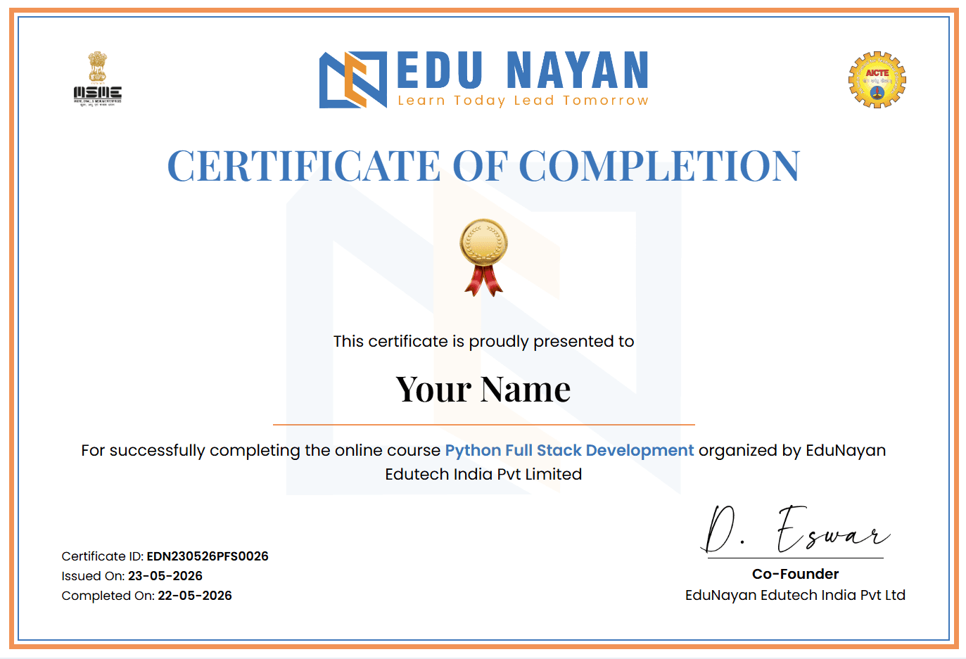
Your Certificate
Earn an industry-recognized certificate upon completion
Official certificate for VLSI Design & Semiconductor Engineer
A shareable completion certificate is issued when you finish the course requirements successfully. Use it on LinkedIn, portfolios, and job applications.
Student Reviews
“The VLSI Design & Semiconductor Engineer course at EduNayan was a turning point for me. The practical curriculum and mock interview support gave me the tools to build actual solutions.”
“Hands-on labs and direct mentorship in the VLSI Design & Semiconductor Engineer program were incredibly helpful. It is fully aligned with modern industry trends.”
Frequently Asked Questions
Quick answers about the course
What will I learn in the VLSI Design & Semiconductor Engineer course?
In this program, you will gain hands-on expertise in VLSI Design & Semiconductor Engineer, covering core theoretical foundations, tool setups, practical exercises, and portfolio-grade capstone projects.
Do I need prior experience to enroll?
No, this course is structured to guide you from basic concepts up to advanced implementations. Having a fundamental understanding of logical thinking is helpful.
Will I receive a certificate?
Yes, on successfully completing the course requirements and capstone projects, you will receive an industry-recognized completion certificate from EduNayan.
What kind of support is available during the course?
You will have access to expert mentors for doubt clearing, step-by-step lab guidance, and dedicated support channels for troubleshooting project errors.